
VTR Architecture Reference XML
架构描述
顶级标签(<arichitecture>)
首先整体架构使用标签< architectures >,该标签包含如下标签:
- < models >
- < tiles >
- < layout >
- < device >
- < switchlist >
- < segmentlist >
- < directlist >
- < complexblocklist >
识别BLIF模型(<models>)
<models>标签包含<model name="string" never_prune="string"> <model>标签。其中每个标签都描述了 FPGA 架构接受的 BLIF .subckt模型名称。模型名称必须与对应的 BLIF 模型名称匹配。
never_prune 标志是可选的,可以是:
- false(默认):裁剪掉没有输出的模块
- true:不裁剪没有输出的模块
默认情况下接受标准 blif 结构 ( .names, .latch, .input, .output),因此这些模型不应在
每一个model标签必须包含两个标签<input_ports> 和 <output_ports>.其中每一个又都包含<port>标签。<port name="string" is_clock="{0 | 1} clock="string" combinational_sink_ports="string1 string2 ..."/>,其属性如下:
- name-端口名字
- is_clock(可选标签)-标识端口是否为时钟,默认值为0
Primitive Timing Modeling Tutorial将is_clock用于对时钟控制模块进行建模,例如时钟发生器、时钟缓冲器/门和时钟多路复用器。
- clock-指定一个端口是序列的(sequential),并由指定的时钟控制(某个is_closk=1的port标签),默认值:端口被对待为组合(combinational)
- combinational_sink_ports-以空格分隔的输出端口列表,这些输出端口组合连接到当前输入端口。默认值:为组合连接(如果未指定)
1 | <models> |
对于上述的single_port_ram,端口we addr data和out都是序列的,因为都指定了clock。 addr 和 data 被标识为组合连接到out,这对应到内部的时序路径(addr 和 data输入寄存器与out输出寄存器之间)
全局FPGA信息
<tiles>content</tiles>:此标签内包含一组<pb_type>标签,用于指定功能块的类型以及属性。
<layout>content</layout>:此标签用于指定设备的网格布局。
<device>content</device>:此标签用于指定设备信息。
<switchlist>content</switchlist>:此标签包含一组<switch>,用于指定开关的类型以及属性。
<segmentlist>content</segmentlist>:此标签包含一组<segment>,用于指定线段的类型以及属性
<complexblocklist>content</complexblocklist>:此标签内包含一组<pb_type>标签,用于指定功能块的类型以及属性。
FPGA网格布局(< layout >)
本标签内的有效标签为:
<auto_layout aspect_radio="float">(最多存在一个这个标签),用于定义可自动缩放到所需大小的可缩放设备网格布局。aspect_radio(可选)-设备网络的横纵比(width/height),默认为1.0
<fixed_layout name="string" width="int" height="int">,用于定义具有固定尺寸的设备网格布局(可指定多个)。name-标识网格布局的唯一名称width-设备网格宽度height-设备网格高度
其中每个<auto_layout>或<fixed_layout>标签应包含一组网格位置标签。每个网格位置规范都有一个相关的数字优先级。优先级较高的位置规范会覆盖优先级较低的位置规范。可以使用特殊的块类型指定空网格位置EMPTY。
1.如果一个网格块与另一个具有较高优先级的块部分重叠,则整个较低优先级的块将从网格中删除。
2.除非另有说明,否则所有网格位置都默认为EMPTY。
网格位置标签
< fill type="string" priority="int"/ >
必须标签属性如下:
- type-指定顶级复杂块的类型(pb_type)的名称
- priority-此布局规范的优先及。具有较高优先级的标签会覆盖具有较低优先级的标签。
1 | <!-- Fill the device with CLB blocks --> |

< perimeter type="string" priority="int"/ >
将设备的周长(即边缘)设置为指定的块类型。必须标签属性如下:
- type
- priority
1 | <!-- Create io blocks around the device perimeter --> |

< corners type="string" priority="int"/ >
将设备的角设置为指定的块类型。必须标签属性如下:
- type
- priority
1 | <!-- Create PLL blocks at all corners --> |

< single type="string" priority="int" x="expr" y="expr"/ >
在单个网格位置指定块类型的单个实例。其标签必须属性如下:
- type
- priority
- x-块类型实例的水平位置
- y-块类型实例的垂直位置
1 | <!-- Create a single instance of a PCIE block (width 3, height 5) |

< col type="string" priority="int" startx="expr" repeatx="expr " starty= "expr" incry="expr"/ >
在 处创建指定块类型的列startx。如果repeatx指定了该列将在任何地方重复\(x=startx+k*repeatx\),满足任何正整数\(k\)。如果指定标签来调整高度 > 1 的块的起始位置,starty则通常使用非零值。<perimeter>。其必选参数如下:
- type
- priority
- startx-指定列的水平起始位置的表达式。
其可选参数如下:
- repeatx-指定列的水平重复因子的表达式。
- starty-指定列的垂直起始偏移量的表达式。(默认0)
- incry-一个表达式,指定区域内块实例化之间的垂直增量。(默认h)
1 | <!-- Create a column of RAMs starting at column 2, and |

1 | <!-- Create IO's around the device perimeter --> |

< row type="string" priority="int" starty=" expr" repeaty="expr" startx="expr"/ >
在 处创建指定块类型的行starty。如果repeaty指定了该列将在任何地方重复\(y=starty+k*repeaty\),满足任何正整数\(k\)。如果指定标签来调整宽度 > 1 的块的起始位置,startx则通常使用非零值。<perimeter>。其必选参数如下:
- type
- priority
- starty-指定行的垂直起始位置的表达式。
其可选参数如下:
- repeaty-指定行的垂直重复因子的表达式。
- startx-指定行的水平起始偏移量的表达式。(默认0)
- incry-一个表达式,指定区域内块实例化之间的水平增量。(默认w)
1 | <!-- Create a row of DSPs (width 1, height 3) at |

< region type="string" priority="int" startx="expr" endx="expr repeatx="expr" incrx=" expr" starty="expr " endy ="expr" repeaty="expr" incry="expr "/ >
用指定的块类型填充由 ( startx, starty) 和 ( endx, endy) 定义的矩形区域。如果repeatx指定了区域将在任何地方重复\(x=startx+k_1*repeatx\),对于任何正整数都满足\(k_1\)。如果repeaty指定了区域将在任何地方重复\(y=starty+k_2*repeaty\),对于任何正整数都满足\(k_2\)。其必选参数如下:
- type
- priority
其可选参数如下:
- startx-指定区域(包括)水平起始位置的表达式。(默认0)
- endx-指定区域(包括)水平结束位置的表达式(默认W-1)。
- repeatx-指定列的水平重复因子的表达式。
- incrx-一个表达式,指定区域内块实例化之间的水平增量。(默认w)
- starty-指定区域(包括)垂直起始位置的表达式。(默认0)
- endy-指定区域(包括)垂直结束位置的表达式。(默认H-1)
- repeaty-repeaty – 指定列的垂直重复因子的表达式。
- incry-一个表达式,指定区域内块实例化之间的垂直增量。(默认h)
1 | <!-- Fill RAMs withing the rectangular region bounded by (1,1) and (5,4) --> |

1 | <!-- Create RAMs every 2nd column withing the rectangular region bounded |

1 | <!-- Fill RAMs within a rectangular 2x4 region and repeat every 3 horizontal |

1 | <!-- Create a 3x3 mesh of NoC routers (width 2, height 2) whose relative positions |

整体的网络布局示例
1 | <layout> |

FPGA器件信息
该信息包含在<device>标签当中,其中包含的子标签为:
<sizing R_minW_nmos="float" R_minW_pmos="float"/>(必须要,用于指定面积模型需要的参数)- R_minW_nmos-最小宽度 nmos 晶体管的电阻。此数据仅由 VPR 中内置的面积模型使用。
- R_minW_pmos-最小宽度 pmos 晶体管的电阻。此数据仅由 VPR 中内置的面积模型使用。
<connection_block input_switch_name="string"/>(必须要)input_switch_name-用于指定在
<switchlist>中定义的<switch>的名字,用来连接布线导线和模块的输入引脚(即,输入连接块)。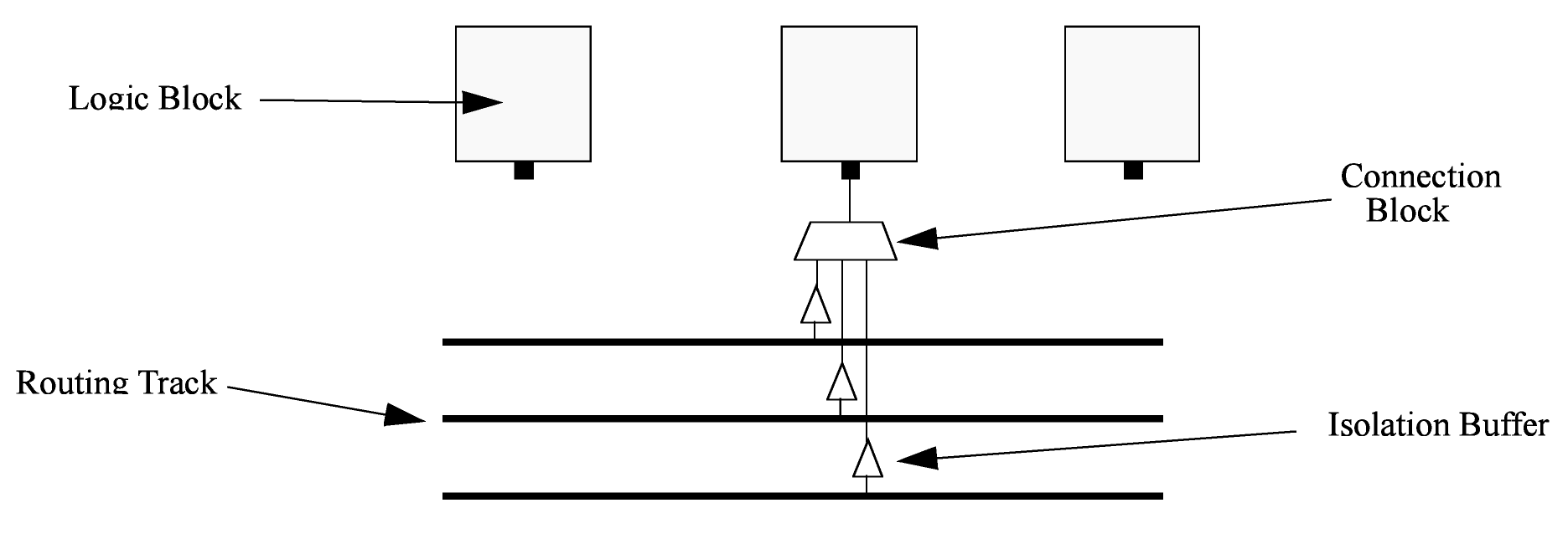
<area grid_logic_tile_area="float"/>(必须要)
指定一个逻辑tile的默认面积(在MWTAs(Minimum Width Transitor Area)下),不包含布线。用于对所有功能块占用的面积进行面积估计。
这个属性会被覆盖,当指定
<switch_block type="{wilton | subset | universal | custom}" fs="int"/>(必须要)- type-指定开关块的类型
- 开关块\(F_s\)的类型
此参数控制用于连接(群集间)路由网段的交换机模式。可以使用单个关键字分别指定三个相当简单的模式,也可以指定更复杂的自定义模式。
没搞明白为什么双向开关的\(F_s\)都是3,而单向开关的\(F_s\)可以是3的整数倍。以及对于穿过开关块的导线是如何处理的
指定
custom允许在<switchblocklist>XML 节点下描述自定义开关块,其格式在Custom Switch Blocks中描述。如果开关块指定为custom,则fs不必指定该字段,如果存在则将被忽略。<chan_width_distr>content</chan_width_distr>此标签内的内容仅在 VPR 处于全局路由模式时使用。该标签的内容在Global Routing Information中描述。
<default_fc in_type="{frac|abs}" in_val="{int|float}" out_type="{frac|abs}" out_val="{int|float}"/>
这定义了默认的 Fc 规范,如果它没有在<fc>顶级复杂块内的标签中指定。这些属性与
开关(switch)
标签<switchlist>中的标签,指定用于将电线和引脚连接在一起的开关。
<switch type="{mux|tristate|pass_gate|short|buffer}" name="string" R="float" Cin="float" Cout="float" Cinternal="float" Tdel="float" buf_size=" {auto|float}" mux_trans_size="float", power_buf_size="int"/>
type-开关的类型
- mux:An isolating, configurable multiplexer
- tristate:An isolating, configurable tristate-able buffer
- pass_gate:A non-isolating, configurable pass gate
- short: A non-isolating, non-configurable electrical short (e.g. between two segments).
- buffer: An isolating, non-configurable non-tristate-able buffer (e.g. in-line along a segment).
isolating:包含一个缓冲器,有助于减少RC延迟。
name-开关的唯一标识
R-开关的电阻
Cin-开关的输入电容
Cout-开关的输出电容
- Cinternal-内部电容(当开关类型为mux或者tristate时,需要指定该参数,因为这两种开关类型都是多个器件级联而成的,由内部电容)
1 | Pass Transistor |
- Tdel-通过开关的固有延迟。如果该开关由零电阻源驱动,并驱动零电容负载,则其延迟将为:\(T_{del}+R\cdot C_{out}\)
- buf_size-以最小宽度晶体管面积 (MWTA) 为单位指定缓冲区大小。(默认值
auto),若设置为auto则根据R的值自动调整大小。 - mux_trans_size-指定
mux类型开关中使用的两级复用器中的每个晶体管的大小(以最小宽度晶体管为单位) - power_buf_size-用于功耗评估,标识buffer相对于最小尺寸反相器的驱动强度
<Tdel num_inputs="int" delay="float"/>
无需指定单个 Tdel 值,而是可以为开关扇入的不同值指定 Tdel 值列表。延迟基于两个最接近的扇入对任何未指定的扇入进行线性外推/插值。
- num_inputs-开关的输入数量
- delay-当开关拓扑具有指定数量的开关输入时的固有开关延迟
1 | <switch type="mux" name="my_mux" R="522" Cin="3.1e-15" Cout="3e-15" Cinternal="5e-15" mux_trans_size="1.7" buf_size="23"> |
全局布线信息
如果要进行全局布线,可以将不同方向和FPGA不同部分的通道设置为不同的相对宽度。这是在<chan_width_distr>标签内的内容中指定的。
如果要执行详细的路由,只能使用均匀分布
暂时不知道干嘛的,先放着,之后再看
物理Tiles
在<tiles>内,描述了FPGA中可用的物理tiles,每一个使用一个<tile>标签指定。
<tile name="string" capacity="int" width="int" height="int" area="float"/>:
- name-tile的唯一标识符
以下为可选参数:
capacity-???没看到相关文档介绍
width-tile在网格中所占的宽度(多少个网格宽度,默认1)
height-tile在网格中所占的高度(多少个网格高度,默认1)
area-逻辑面积(in MWTA)(默认值来源于
<area>)
以下为可用的子标签:
<clock name="string" num_pins="int" equivalent="{none|full}"/>:用于描述时钟端口
<sub_tile name="string" capacity="{int}">(每个tile至少指定一个subtile)
- name-唯一标识符
- capacity-这种类型的块在每个网格上的实例化数量(默认值1)
<input name="string" num_pins="int" equivalent="{none|full}" is_non_clock_global="{true|false}"/>:用于定义输入端口,多个输入端口使用多个此标签。
- name-输入端口名称
- num_pins-输入端口宽度
- equivalent(optional)-引脚是否具有逻辑灯效性
none:没有输入引脚具有逻辑等效性。(如adder)full:所有的输入引脚都具有逻辑等效性。(如lut)
- is_non_clock_global-是否为全局时钟信号
<output name="string" num_pins="int" equivalent="{none|full|instance}"/>::用于定义输出端口,多个输出端口使用多个此标签。
- name-输出端口名称
- num_pins-输出端口的引脚数量
- equivalent(optional)-引脚是否具有逻辑灯效性
nonefullinstance:可以交换块内的子实例(例如 LUT/BLE)的模型,以实现有限形式的输出引脚逻辑等效。
<clock name="string" num_pins="int" equivalent="{none|full}"/>是否为时钟端口
<equivalent_sites>
其子标签如下:
<site pb_type="string" pin_mapping="string"/>- pb_type-对应pb_type的名字
- pin_mapping-指定在物理tile与逻辑pb_type类型之间需要引脚映射(默认direct)
direct:不需要指定pin映射,因为tile pin定义等于对应的pb_typecustom:引脚映射是用户定义的
<direct from="string" to="string">(描述物理tile与pb_type之间的端口映射)form:对应于物理tile的引脚to:对应与逻辑块的引脚
<fc in_type="{frac|abs}" in_val="{int|float}" out_type="{frac|abs}" out_val="{int|float}">
<fc_override fc_type="{frac|abs}" fc_val="{int|float}", port_name="{string}" segment_name="{string}">用于覆盖某个端口的\(F_c\)
- fc_type
- fc_val
- port_name(可选)-此覆盖适用的端口的名称。如果未指定,则此覆盖适用于所有端口。
- segment_name(可选)-此覆盖适用的段的名称(在
<segmentlist>下定义)。如果未指定,则此覆盖适用于所有段。
两个可选参数至少指定一个
<pinlocations pattern="{spread|perimeter|custom}">(没有此标签则默认为spread)
- pattern
spread:表示引脚将均匀分布在复杂块的所有侧面。perimeter:表示引脚将均匀分布在复杂块的周边侧soread_inputs_perimeter_outputs:表示输入引脚将分布在复杂模块的所有侧面,但输出引脚仅分布在模块的周边。custom:允许架构师使用标签<loc>具体指定引脚的放置位置。<loc side="{left|right|bottom|top}" xoffset ="int" yoffset="int">name_of_complex_logic_block.port_name[int:int] ... </loc>- side-位于grid的哪一个边
- xoffset(可选,0)-指定从块原点(左下角)的水平偏移(以网格为单位)。偏移值必须小于块的宽度。
- yoffset(可选,0)-指定距块原点(左下角)的垂直偏移量(以网格为单位)。偏移值必须小于块的高度。
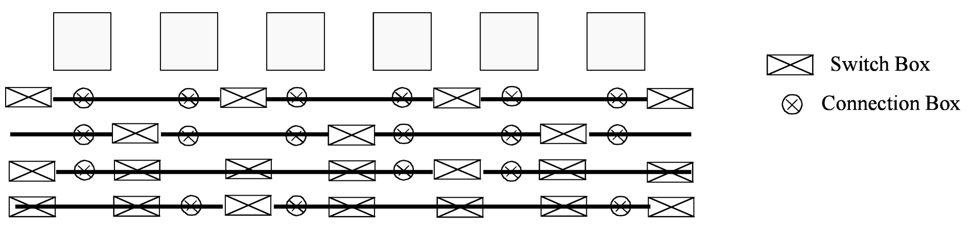
<switchblock_locations pattern="{external_full_internal_straight|all|external|internal|none|custom}" internal_switch="string">:描述与复杂块相关的全局路由交换块的创建位置。(如果未指定,则假定未默认模式)
pattern(默认值为第一个)
external_full_internal_straight:在复杂块外部创建完整的开关块,在复杂块内创建直接的开关块all:在路由通道交叉的地方创建开关块external:在路由通道在复杂块之外的任何地方创建开关块internal:在复杂块内路由通道交叉的任何地方创建开关块none:表示没有为复杂块创建切换块custom:允许架构师使用<sb_loc>标签指定自定义开关块位置和类型

internal_switch:来自
<switchlist>,应用于内部开关块的开关名称(Default: The default switch for the wire<segment>)
1 | <switchlist> |
子标签:
<sb_loc type="{full|straight|turns|none}" xoffset="int" yoffset="int", switch_override="string">:当选择custom属性时,指定开关块的位置
type(默认full)-指定开关块的类型
full:表示将创建一个完整的开关块straight:表示将创建一个只有直通连接的开关块turns:表示将创建一个只有转向连接的开关块none:表示不会创建 switchblock

xoffset(可选,0)-指定从块原点(左下角)的水平偏移(以网格为单位)。偏移值必须小于块的宽度。
yoffset(可选,0)-指定距块原点(左下角)的垂直偏移量(以网格为单位)。偏移值必须小于块的高度。
switch_override-创建开关块所使用的开关名字(from
<switchlist>)(Default: The default switch for the wire<segment>)
The switchblock associated with a grid tile is located to the top-right of the grid tile
如果我们假设一个宽度=2、高度=3 的块,我们可以使用自定义模式来指定等效于“电气短路内部直连”示例的架构:
1 | <switchblock_locations pattern="custom"> |
复杂块
<complexblocklist>中的内容描述了 FPGA 中的复杂模块。<complexblocklist>内每种类型的复杂块都使用标签内的顶级标签<pb_type>指定。
PB_Type
<pb_type name="string" num_pb="int" blif_model="string"/>:用于指定最顶层的复杂块,或者复杂块内部的部件(sub_blocks),使用哪些属性,取决于该标签在层次结构中的位置。
- 顶层(Top Level):
<complexblocklist>的子标签 - 中间(Intermediate):一个
<pb_type>的子标签 - 基元(Primitive/Leaf):不包含
<pb_type>子标签
1 | <complexblocklist> |
name-pb_type的名字,相对于其父节点、同级节点以及子节点都应该是唯一的
num_pb-当前pb_type在此层次结构中实例化的数量(默认1)
1 | <!--CLB包含10个BLE--> |
blif_model-指定此pb_type所实现的网表基元
.input:A BLIF netlist input.output:A BLIF netlist output.names:A BLIF .names (LUT) primitive.latch:A BLIF .latch (DFF) primitive.subckt <custom_type>:A user defined black-box primitive.
class-指定这个原语是一个特殊的类型,应该被特殊对待。
1 | <pb_type name="my_adder" blif_model=".subckt adder"/> |
pb_type基元的输入、输出以及时钟端口必须与<models>中指定的对应
适用于所有< pb_type >标签的子标签:(与物理tile的描述很相似)
<input name="string" num_pins="int" equivalent="{none|full}" is_non_clock_global="{true|false}"/>:定义输出端口,多个输入端口使用多个标签。
<output name="string" num_pins="int" equivalent="{none|full|instance}"/>
<clock name="string" num_pins="int" equivalent="{none|full}"/>
<mode name="string" disable_packing="bool">:为pb_type指定一个操作模式,每一个子model标签标识一个不同的操作模式,每一个<pb_type>和<interconnexct>标签。
- name-唯一标识符
- disable_packing-用于指定该模式是否diable,或者不用于VPR打包器,一般用于调式用
1 | <!--A fracturable 6-input LUT--> |
interconnect
<model>标签的子标签<interconnect>包含以下子标签:
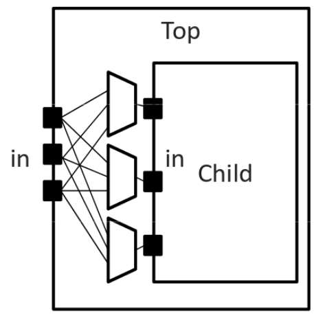
<complete name="string" input="string" output="string">:描述一个全连接crossbar——任何输入都可以连接到任何输出。
- name-互联标识符
- inout-输入到互联的引脚
- output-输出到互联的引脚
1 | <complete input="Top.in" output="Child.in"/> |
<direct name="string" input="string" output="string"/>:在输入和输出之间描述一个一对一映射。
- name-互联标识符
- input-输入引脚
- output-输出引脚
1 | <direct input="Top.in[2:1]" output="Child[1].in"/> |

<mux name="string" input="string" output="string"/>:描述一个基于总线的多路选择器。
- name
- input
- output
1 | <mux input="Top.A Top.B" output="Child.in"/> |

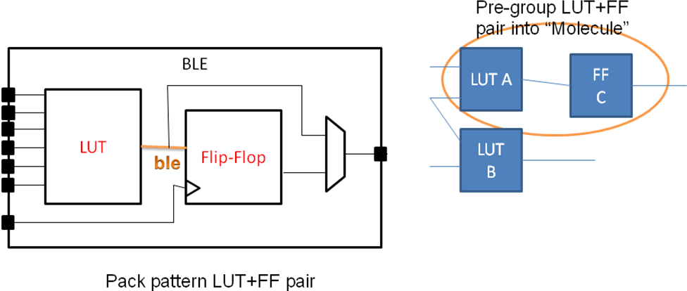
上述三个标签都有一个可选的子标签<pack_pattern name="string" in_port="string" out_port="string"/>,使得CAD在打包的时候能将用到该两个元件的时候,能够打包到一起。
- name-标识符
- in_port-输入引脚
- out_port-输出引脚
下面的例子就可以让CAD在打包的时候,如果遇到一个LUT后面连接一个触发器,则会将其打包在一个BLE当中。
1 | <pack_pattern name="ble" in_port="lut.out" out_port="ff.D"/> |
Classes
calss是基元<pb_type>的可选属性,使得指定那些常见的基元更加方便,内置的class可选值为:
用于描述一个K-LUT(所有哦输入引脚都逻辑等效),当这个类型被使用时,输入段楼必须有属性port_class="lut_in",并且输出端口必须有属性port_class_"lut_out"。
描述一个触发器。其输入端口必须要有属性port_class="D",输出端口必须要有属性port_class="Q",时钟端口必须要有属性port_class="clock"。
描述一个存储器,存储器是很特殊的,因为一个存储器可以包含多个更小的逻辑存储器,只要满足以下条件:
- 地址、时钟以及控制输入是相同的
- 当不同的的网表存储器合并成一个物理存储器时,存在足够的物理数据管脚来满足网表存储器的需求。
不同类型的存储器所需要的属性不一样。
单端口存储器:
- input 端口
port_class="address"port_class="data_in"port_class="write_en"
- output 端口
port_class="data_out"
- clock 端口
port_class="clock"
双端口存储器:
- input 端口
port_class="address1"port_class="data_in1"port_class="write_en1"port_class="address2"port_class="write_en2"
- output 端口
port_class="data_out1"port_class="data_out2"
- clock 端口
port_class="clock"
Timing
时序是通过包在pb_type、complete、direct、mux中的标签来指定的。
<delay_constant max="float" min="float" in_port="string" out_port="string"/>:用于指定从输入端口到输出端口的最大以及最小延迟。
不太明白,如果自定义单元的输入端口与输出端口之间很复杂(可以选择是否有寄存器),那么延迟该如何定义?
可选参数如下:(两者至少包含一个)
- max-最大延迟值
- min-最小延迟值
必须参数如下:
- in_port-输入端口名字
- out_port-输出端口名字
如果in_port与out_port之间是组合逻辑,则该标签指定的是输入与输出之间的组合逻辑延迟。如果in_port与out_port之间是时序逻辑,则该标签指定的是输入寄存器和输出寄存器之间的组合逻辑延迟。
<delay_matrix type="{max | min}" in_port="string" out_port="string"> matrix </delay>:用于描述输入端口与输出端口之间所有引脚的之间的延迟,矩阵的行数与输入数量一致,矩阵的列数与输出的个数一致。
1 | <delay_matrix type="max" in_port="in" out_port="out"> |
<T_setup value="float" port="string" clock="string"/>:指定端口寄存器的建立时间约束。(仅仅只用于 primitive pb_type tags)
<T_hold value="float" port="string" clock="string"/>:指定端口寄存器的保持时间约束。(仅仅只用于 primitive pb_type tags)
<T_clock_to_Q max="float" min="float" port="string" clock="string"/>:指定端口寄存器的保持时间约束。(仅仅只用于 primitive pb_type tags)
对时序基元的内部时序路径进行建模
1 | <pb_type name="seq_foo" blif_model=".subckt seq_foo" num_pb="1"> |
为了模拟内部关键路径延迟,我们指定输入寄存器的内部时钟到 Q 延迟 (10ps)、内部组合延迟 (0.9ns) 和输出寄存器的建立时间 (90ps)。这些延迟的总和对应于 1ns 的关键路径延迟。
Power
<power method="string">contents</power>
method-用于指明功耗评估的方式(default:auto-size)
specify-sizeauto-sizepin-toggleC-internalabsoluteignoresum-of-children
contents则可以包含以下标签:
<dynamic_power power_per_instance="float" C_internal="float"/>
<static_power power_per_instance="float"/>
<port name="string" energy_per_toggle="float" scaled_by_static_prob="string" scaled_by_static_prob_n="string"/>
Wire Segments
根节点为<segmentlist>,其内容为一组<segment>标签组成。
<segment axis="{x|y}" name="unique_name" length="int" type="{bidir|unidir}" freq="float" Rmetal="float" Cmetal="float">content</segment>
可选标签:
- axis-指定线段是只用于x通道还是只用于通道,如果未指定,则x、y通道都可以使用。
需要的标签:
- name-独一无二的线段类型的名字
- length-要么是标识线段长度(穿过多少个逻辑块),或者为关键字
longline(跨过整个FPGA阵列) - freq-此类线段在通道中所占的权重(该值除以所有线段该值的和)。
- Rmetal-每单位长度(以逻辑块为单位)的电阻(欧姆)
- Cmetal-每单位长度(以逻辑块为单位)的电容(法拉)
- directionality-线段的方向性。表明一个线段是否有多个驱动点(双向),或者线段的一端有一个驱动器(单向)(所有线段必须有相同的方向性值)
- content-包含开关名称、连接块填充以及开关块填充
content中的可用标签:
<sb type="pattern">int list</sb>
<cb type="pattren">int list</cb>
上述两个标签用于指定开关块以及连接块的填充性质,不能用于longline segments,因为该类型的线段被指定为全部填充。
自定义开关块
1 | <switchblocklist> |
<switchblock name="string" type="string">
<switchblock> 是描述不同线段类型之间连接的顶层XML文件,有以下属性:
- name – A unique alphanumeric string
- type –
unidirorbidir.
<switchblock_location type="string"/>
Required Attributes
type –Can be one of the following strings:
EVERYWHERE– at each switch block of the FPGAPERIMETER– at each perimeter switch block (x-directed and/or y-directed channel segments may terminate here)CORNER– only at the corner switch blocks (both x and y-directed channels terminate here)FRINGE– same as PERIMETER but excludes cornersCORE– everywhere but the perimeter
在 FPGA 上设置此开关块所描述的连接将被实例化的位置。